
 By
By 
A nanotech camera is an imaging device that uses nanotechnology, either in its sensor construction or optical components, to capture light and detail at scales far smaller than conventional cameras allow. These innovations typically involve structures measured in billionths of a meter, engineered to manipulate light in ways that traditional silicon-based sensors and glass lenses cannot.
For photographers in 2026, this matters because nanotech is already changing what your camera can do. Sensors built with nanowire arrays can capture a wider dynamic range in a single exposure. Metasurface lenses, thinner than a human hair, are replacing bulky glass elements in smartphone cameras and specialized imaging systems. What once required a full-frame sensor and premium glass can now fit inside devices you’d barely notice.
The practical upside? Better low-light performance, smaller form factors without sacrificing image quality, and new capabilities like hyperspectral imaging that reveals details invisible to the naked eye. You’re seeing this tech trickle into consumer cameras, medical imaging, and even surveillance systems where size and sensitivity are everything.
This article breaks down how nanotech cameras actually work, the specific types of nanotechnology reshaping sensors and optics, and where you’ll encounter these systems in real-world photography. Whether you’re weighing a new camera purchase or just curious about the science pushing the boundaries of imaging, understanding nanotech helps you make sense of what manufacturers are promising and what’s genuinely useful versus marketing hype.
What a Nanotech Camera Actually Means
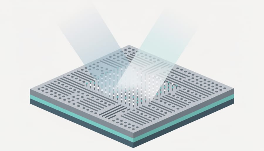
A nanotech camera isn’t a distinct product category, it’s any camera whose image sensor incorporates nanotechnology to improve performance. The “nano” prefix refers to engineering at the nanometer scale, where structures measure between 1 and 100 billionths of a meter. At this microscopic level, materials behave differently than they do in bulk, allowing engineers to manipulate how light interacts with sensor components in ways that weren’t possible with conventional manufacturing.
Traditional camera sensors rely on relatively straightforward silicon photodiodes arranged in a grid. Light passes through color filters and microlenses before hitting these photodiodes, which convert photons into electrical signals. While this design has improved dramatically over decades, it faces physical limits, particularly in how efficiently each pixel captures light and how accurately it distinguishes colors.
Nanotech sensors break past some of these barriers by embedding nanoscale structures directly into the sensor architecture. These might include quantum dots that convert specific wavelengths more efficiently, nanostructured surfaces that reduce reflection and crosstalk between pixels, or plasmonic materials that concentrate light into smaller areas. The key terms you’ll encounter include:
- Nanometer
- One billionth of a meter, the scale at which materials exhibit quantum mechanical properties useful for manipulating light.
- Quantum Dot
- A semiconductor nanocrystal that emits or absorbs specific wavelengths based on its size, enabling more precise color filtering than traditional dyes.
- Photonic Nanostructure
- Engineered patterns at the nanoscale that control how light waves propagate, reflect, or concentrate within the sensor.
- Plasmonic Filter
- A metallic nanostructure that uses surface plasmons to selectively transmit certain colors while blocking others, replacing conventional absorptive filters.
The practical result is sensors that gather more light per pixel, distinguish colors more accurately, and generate less noise, especially in challenging conditions like low light or high contrast scenes. Not every camera marketed with nanotech benefits uses the same approach, so the performance gains vary widely depending on which nanoscale innovations a manufacturer has actually implemented.
How Nanotech Camera Sensors Work
Light Capture at the Nanoscale
At the heart of a nanotech camera sensor is a fundamentally different relationship with light. Traditional silicon pixels capture photons through a straightforward process, light hits the photodiode, converts to electrical charge, and gets measured. But at the nanoscale (structures smaller than the wavelength of visible light itself), physics starts behaving differently.
Nanostructured surfaces can trap and channel light with remarkable precision. Instead of photons bouncing off silicon or passing through inefficiently, engineered nanopatterns act like microscopic funnels. These structures, often arrays of nano-pillars or precisely etched gratings, guide more light directly into the active sensor area. The result? You capture a higher percentage of incoming photons, which translates to better performance in dim conditions without cranking up ISO.
Crosstalk, where light meant for one pixel bleeds into neighbors and muddies color accuracy, gets significantly reduced too. Conventional sensors rely on simple barriers between pixels, but photons don’t always respect those boundaries. Plasmonic materials (metals engineered at the nanoscale to interact with specific light wavelengths) can create sharper boundaries that keep light where it belongs.
Color filtering sees perhaps the most dramatic change. Standard sensors use dyed polymer filters placed above each pixel, an approach that wastes much of the light it blocks. Quantum dots, tiny semiconductor nanocrystals, can replace these filters. They absorb light and re-emit it at precise wavelengths determined by their size, delivering purer colors while maintaining higher light transmission. Some designs skip traditional Bayer patterns entirely, letting each pixel capture fuller color information through layered quantum dot structures.
The payoff extends beyond raw sensitivity. You get cleaner color separation, less moiré, and better edge definition, all because the sensor is working with light at its most fundamental scale.
From Photons to Pixels: The Nanotech Advantage
When a photon enters a camera, it begins a journey that transforms pure light into digital information. In traditional camera sensor tech this process involves light passing through color filters and microlenses before striking silicon photodiodes that convert photons to electrons. The efficiency of this conversion determines how much light you actually capture versus how much gets wasted as heat or reflection.
Nanotech sensors reimagine this pathway at the molecular level. Instead of relying solely on traditional color filter arrays that block roughly two-thirds of incoming light, nanoscale structures can actively channel and sort photons with far less waste. Quantum dots, for instance, absorb specific wavelengths and re-emit them directly to the photodiode beneath, bypassing the light-blocking approach of Bayer filters. This means more photons translate into usable signal rather than being discarded.
The electron conversion stage gets an upgrade too. Nanostructured surfaces increase the effective capture area of each photosite without enlarging the physical pixel. Think of it as creating microscopic funnels that guide stray photons toward the sensor’s active regions instead of letting them scatter into neighboring pixels or dead zones. This reduces crosstalk, the phenomenon where light meant for one pixel bleeds into another and creates false color or softness.
Where this matters most is in the final image data. Higher quantum efficiency means you need less amplification to reach proper exposure, which directly translates to lower noise at high ISO settings. Wider dynamic range comes from capturing subtler variations in electron count before clipping highlights or losing shadow detail. Compared to conventional CMOS or CCD sensors nanotech implementations squeeze measurably more information from the same amount of incoming light, giving you cleaner files with richer tonal gradations straight out of the camera.
Types of Nanotechnology Used in Camera Sensors
Quantum Dot Technology
Quantum dots are semiconductor nanocrystals, typically 2-10 nanometers across, that absorb light and re-emit it at very precise wavelengths determined by their size. In camera sensors, manufacturers place quantum dot layers above traditional photodiodes to convert incoming light into wavelengths the silicon below can capture more efficiently.
This approach solves a longstanding problem: silicon sensors struggle with certain colors, particularly deep reds and blues, because photons at those wavelengths either penetrate too deeply or bounce off the sensor surface. Quantum dots intercept these difficult wavelengths and convert them to green light, which silicon captures best. The result is more accurate color reproduction across the spectrum and improved sensitivity in challenging lighting.
Samsung’s ISOCELL sensors for smartphones use quantum dot color filters instead of conventional Bayer filters, reducing crosstalk between pixels and boosting light transmission by roughly 30 percent. Sony has explored similar quantum dot implementations in their mirrorless camera sensor research, though widespread adoption in full-frame sensors remains in development. The technology delivers the most dramatic improvements in compact sensors where pixel size constraints traditionally limited performance.

Nanostructured Light Management
Nanostructured light management tackles one of the fundamental challenges in sensor design: getting photons where they need to go without losing them along the way. Traditional sensors waste a significant portion of incoming light to reflection, scattering between pixel boundaries, and absorption by the wrong photodiode. Nanotech approaches reshape the physical architecture of the sensor surface to control light’s path at scales smaller than the wavelengths themselves.
Plasmonic filters use precisely engineered metal nanostructures that resonate with specific light wavelengths. Instead of conventional dye-based color filters that absorb unwanted colors (converting that light to heat), plasmonic filters redirect photons through interference effects. This means more light reaches the photodiodes, improving quantum efficiency especially in low-light conditions. Canon and Samsung have both filed patents describing plasmonic implementations that could boost sensitivity by 30-40% compared to Bayer filters.
Nano-patterned surfaces work similarly to a microscopic funnel array. Engineers etch patterns measured in hundreds of nanometers onto the sensor’s protective glass or directly onto pixel structures. These patterns reduce reflections that would normally bounce light back out of the camera, and they help guide oblique rays toward the center of each photodiode rather than letting them hit the metal wiring between pixels.
Microlens enhancements represent the most mature nanostructured approach already shipping in cameras today. Modern sensors stack multiple layers of progressively smaller lenses above each pixel, with the top layer shaped using nanoimprint lithography to create aspherical profiles that would be impossible at larger scales.
Emerging Nanomaterials
Beyond the nanotech solutions already in cameras, researchers are testing materials that could redefine how sensors capture light. Graphene, a single-atom-thick carbon sheet, shows promise for ultra-sensitive imaging because electrons move through it almost without resistance. Early graphene sensor prototypes detect a broader spectrum than silicon can manage, potentially matching what specialized infrared sensors do while also seeing visible light. Perovskite nanocrystals, meanwhile, offer tunable absorption properties; by adjusting their composition, engineers can optimize them for specific colors or wavelengths, which could eliminate traditional Bayer filters entirely. Neither technology has reached commercial cameras yet, graphene integration remains expensive, and perovskites degrade under prolonged exposure, but pilot studies hint at sensors that combine extreme sensitivity with remarkable dynamic range. If manufacturing hurdles fall, these materials may power the next leap in low-light and computational photography.
Where Nanotech Cameras Are Being Used Today

Consumer Photography
Nanotech enhancements have moved from research labs into the cameras you can actually buy. Smartphone makers adopted quantum dot sensors first, squeezing more light sensitivity into tiny pixels packed onto fingernail-sized chips. Apple’s recent iPhone models use nano-patterned color filters that reduce crosstalk between adjacent pixels, yielding cleaner images when you shoot indoors or after sunset. Samsung and Google employ similar nanoscale tricks to boost dynamic range, letting you capture both bright skies and shadowed foregrounds in a single frame without blown highlights.
Mirrorless camera bodies now incorporate nanostructured microlenses that funnel stray light back toward photodiodes instead of letting it scatter. Canon and Sony sensors with these refinements deliver noticeably better high-ISO performance, meaning less grain at settings like 6400 or 12800. That sensor magic translates directly into sharper concert shots and wildlife photos at dawn without needing a tripod.
Computational photography leans heavily on nanotech gains. Because quantum dot sensors capture more accurate color data from the start, your phone’s software doesn’t have to guess as much when stacking exposures or applying Night Mode. The hardware foundation matters: better raw input means smart camera features like AI subject tracking and real-time HDR preview work faster and more reliably, giving you clean results straight out of the camera.
Professional and Scientific Applications
Beyond consumer photography, nanotech sensors excel in specialized fields where conventional imaging hits its limits. Medical endoscopy systems increasingly rely on quantum dot sensors that capture infrared and near-infrared wavelengths invisible to traditional cameras, helping surgeons identify tissue boundaries and blood flow patterns during minimally invasive procedures. These same wavelengths matter for dermatology imaging, where subsurface skin analysis requires sensitivity beyond what standard CMOS sensors deliver.
Astrophotography pushes sensor technology harder than almost any other discipline. Telescope-mounted cameras using nanostructured pixels can detect individual photons from distant galaxies, pulling detail from near-total darkness. The reduced thermal noise from nanoscale engineering means shorter cooling times and longer exposure stability, critical for deep-sky imaging where exposures stretch across hours. Some observatory-grade sensors now incorporate plasmonic filters that isolate specific emission lines from nebulae without external filter wheels, simplifying optical setups.
Industrial inspection systems exploit nanotech sensors for quality control tasks that demand both speed and precision. Manufacturing lines use cameras with nano-engineered spectral response to detect material defects, coating thickness variations, and contamination invisible under standard lighting. Semiconductor fabrication relies on these sensors to inspect wafer surfaces at resolutions where nanometer-scale defects can ruin entire production runs. The technology’s ability to work across ultraviolet, visible, and infrared spectra simultaneously makes it invaluable where traditional multi-camera setups would be impractical.
What Nanotech Means for Your Photography
The most immediate benefit you’ll experience with a nanotech-enhanced sensor is cleaner high-ISO shooting. Those same family dinner shots that looked grainy at ISO 3200 on your older camera now stay sharp and noise-free at ISO 6400 or even 12800. This isn’t theoretical improvement. You can push your camera two or three stops further before image quality suffers, which translates directly to shooting in dimmer venues without a flash or capturing faster-moving subjects without motion blur.
Color accuracy sees real gains too. Quantum dot filters separate wavelengths more precisely than traditional Bayer arrays, so skin tones look natural without extensive color correction in post. Blues stay blue instead of shifting purple, and reds don’t clip as easily in mixed lighting. If you’ve ever struggled with fluorescent or LED color casts, sensors with nanoscale color management handle these situations with less fuss.
Sensor size matters less than it used to. Nanostructured photodiodes extract more usable signal from each photon, which means smaller sensors can now match performance that previously required larger formats. This shift enables genuinely pocketable cameras with image quality that would have needed a DSLR body five years ago.
Will you notice the difference if you’re upgrading from a decent three-year-old camera? Maybe not in bright daylight at base ISO. The gap shows up when conditions get difficult: twilight cityscapes, indoor sports, backlit portraits. That’s where enhanced light capture and reduced noise become visible advantages rather than spec sheet footnotes.
When shopping, look past marketing buzzwords. Check actual ISO performance tests, examine real-world sample images in challenging light, and compare dynamic range measurements. Not every “advanced sensor technology” claim involves meaningful nanotech implementation. Focus on measurable improvements in the shooting scenarios you care about rather than chasing the newest label.
Common Questions About Nanotech Cameras
Switching to a camera with a nanotechnology-enhanced sensor feels like a big decision, especially when you’re trying to separate genuine innovation from marketing hype. Here are the questions photographers most often ask about this technology, along with straightforward answers.
Are nanotech sensors more expensive than conventional sensors?
Currently, cameras with nanotech-enhanced sensors typically cost slightly more than equivalent conventional models, but the premium has narrowed significantly as manufacturing scales up. In many mid-range smartphones and mirrorless cameras, the cost difference is negligible because manufacturers absorb it across their production volume.
Do nanotech sensors require special care or maintenance?
No, they don’t need any special handling beyond normal sensor care. The nanostructures are integrated into the sensor substrate itself, so cleaning and protection work exactly the same as with traditional sensors.
Will nanotech sensors completely replace traditional CMOS and CCD designs?
Not entirely. Rather than wholesale replacement, nanotechnology is being layered onto existing sensor architectures to enhance their performance. Most “nanotech cameras” still use CMOS or BSI-CMOS foundations with nanostructures added for light management, color filtering, or sensitivity gains.
How do nanotech-enhanced sensors compare to larger traditional sensors in full-frame cameras?
Sensor size still matters fundamentally for depth of field, light-gathering area, and resolution potential. Nanotechnology helps smaller sensors punch above their weight in low-light performance and color accuracy, but it can’t replicate the physics of a larger sensor’s total light collection or background blur characteristics.
One concern that comes up frequently is whether this technology has been proven reliable over time. The answer depends on which type of nanotech we’re discussing. Quantum dot color filters, for instance, have been shipping in consumer cameras since 2019 and have shown stable performance across millions of units. More experimental approaches like graphene sensors remain in research phases, so they’re not something you’ll encounter in commercial products yet.
Compatibility with your existing lenses is straightforward because the sensor enhancements happen at the silicon level, not the lens mount. Your lenses attach and communicate with the camera body exactly as they always have. The nanotech improvements are entirely internal to the sensor itself, affecting image quality but not mechanical or electronic lens communication.
If you’re deciding whether to buy a camera with nanotech features today, consider your actual shooting needs. For low-light work, astrophotography, or situations where you need maximum dynamic range from a compact body, the technology delivers measurable benefits. For studio work with controlled lighting or landscapes shot at base ISO, the advantages become less pronounced, though improved color accuracy can still matter.
Nanotech cameras represent a fundamental shift in how sensors capture light, moving beyond traditional silicon architectures to manipulate photons at the molecular level. By incorporating quantum dots, plasmonic filters, and nanostructured surfaces, these sensors deliver measurable improvements in low-light performance, color accuracy, and dynamic range without requiring physically larger sensors.
What started as experimental lab work has quietly entered mainstream photography. Your smartphone likely already uses some form of nanotechnology in its imaging stack, whether through quantum dot color filters or nano-patterned microlenses. As this technology matures and manufacturing costs drop, you’ll see these innovations migrate from flagship devices into mid-range cameras and specialized applications where extreme sensitivity matters.
The evolution from film to digital took decades. The transition from conventional CMOS sensors to nanotech-enhanced imaging is happening faster but follows a similar pattern, early adopters first, then gradual mainstream integration. We’re currently in that middle phase where the technology works reliably but hasn’t yet reached its full potential.
If you’re shopping for a camera today, understanding nanotech gives you realistic expectations about what sensors can deliver. You don’t need to chase the latest nanotech marketing claims, but recognizing these fundamentals helps you evaluate whether specific performance improvements justify the price premium. Keep watching this space. The next few years will bring refinements that make today’s cutting-edge sensors look conservative by comparison.




 By
By